


Crystals may seem perfect in textbooks, but in the real world, they’re far from flawless. Atomic defects—tiny irregularities in the structure—can have dramatic effects on material properties like conductivity, strength, and color. For molecular modelers and materials scientists, simulating and visualizing these imperfections is a key challenge. If you’re working with crystalline materials, have you ever asked yourself: How can I study the impact of defects on crystal structure?
In this post, we’ll walk through how to model and visualize defects in a diamond crystal using the Crystal Creator Extension in SAMSON, the integrative molecular design platform. This hands-on approach allows you to inspect how atomic occupancy affects the overall geometry of a crystal, in just a few steps. Whether you’re teaching solid state chemistry or developing new materials, this tool can offer meaningful insights.
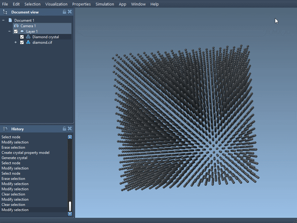
Getting Started: The Perfect Diamond
First, you’ll need a clean diamond crystal structure to use as the basis for comparison. You can download a diamond CIF file (Crystallographic Information File) from databases such as RRUFF or American Mineralogist Crystal Structure Database. Once you have your file:
- Open SAMSON and launch the Crystal Creator App (via Home > Apps > Materials > Crystal Creator).
- Load the CIF file. A window will open allowing you to select settings like number of unit cells and whether to visualize the mesh.
- Make sure to click Open to load the structural model into your data graph.
Once imported, you can generate bonds using SAMSON’s built-in interaction models (such as the Brenner potential) and minimize the structure to prepare it for comparison.
Introducing a Defect
Now comes the interesting part: introducing a vacancy-type defect. Duplicate your CFA file and open it in a text editor. Near the end of the file, locate the section declaring atomic positions. It may look like this:
|
1 2 3 4 5 6 |
loop_ _atom_site_label _atom_site_fract_x _atom_site_fract_y _atom_site_fract_z C 0.00000 0.00000 0.00000 |
To simulate a defect, replace it with the following:
|
1 2 3 4 5 6 7 |
loop_ _atom_site_label _atom_site_fract_x _atom_site_fract_y _atom_site_fract_z _atom_site_occupancy C 0.00000 0.00000 0.00000 0.95 |
This indicates that the atom at this site has a 95% chance of appearing—i.e., there’s a 5% vacancy rate at that position.
Compare and Observe
After saving your modified file:
- Re-open the new CIF file with the Crystal Creator App in SAMSON.
- Generate bonds again and minimize the structure.
- Visually compare the new model with the original to note structural distortions.
You’ll notice that subtle vacancies can result in visible changes in the crystal lattice. If you’re examining mechanical, optical, or electronic properties, such changes might provide valuable clues about system behavior at the atomic scale.
Why This Matters
Defects are essential to understanding real-world materials. From semiconductors with deliberate dopants to natural gemstones with slight imperfections, minor variations influence function in major ways. Using this method, you can test how different occupancies affect your models and potentially set up simulations for further studies.
For more guidance and advanced customization options—including modeling defect distributions and creating your own crystals—visit the full documentation at SAMSON Crystal Creator documentation.
SAMSON and all SAMSON Extensions are free for non-commercial use. You can get SAMSON at https://www.samson-connect.net.